5. Structural Level Design |
What is Structural Level DesignFrom a conceptual point of view, structural level design is the simplest. The easiest way to design gate level logic is in fact to build its structure from components. So we are going to implement a serial in - parallel out shift register this way here. Like in the previous exercise, the clock will be controlled by a slide switch, and the input by a push button. Each of the wires that form part of the output 8-bit bus will be connected to one of the LEDs. So what does it look like? Well very much like this: Looking at this image, all we really need are 8 instances of a D-Type flip flop wired up correctly. Now we could code each of these up individually, but this is time consuming and error prone, so instead we will use modular design and code reuse to reduce the complexity and size of the task at hand. |
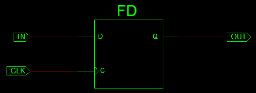
Time to Start CodingLoad the Xilinx ISE development environment and load up your previous project (the one where you made a D-Type flip-flop). We are going to slightly edit and then re-use this module within our new one. Remove the current user constraints file that is attached to the D-type module by right clicking on it and selecting remove. Then, if it is not already open, double click on the remaining file to open it. Notice that all the D-Types in the image do not have inverted outputs (QBar). This is fairly standard for most digital design, where data is just required to be held between clock edges, not inverted and held. Also remember that because of this trend, the synthesis tool created two D-Types to control Q and QBar, not one. Therefore our first step is to remove QBar from the module. Once you have removed all traces, synthesise your module and look at its RTL schematic. There are several things to watch out for when removing QBar. You will make these mistakes often so get used to it...
The schematic should show a single D-Type flip-flip (named FD, which is Xilinx shorthand for Flipflop Dtype). Congratulations, you now have your very own D-type. |
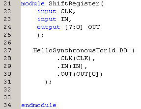
The Top Level ModuleNow that you have a D-Type, it is time to create your top level module that will represent your shift register. Create a new Verilog module called "ShiftRegister" with the following inputs and outputs, and make this your top level module.
Now we need to fill in our empty module by instantiating several of our D-Types. Until a module is instantiated within the hierarchy of the top level module, it should be considered more of a blueprint. You have already seen instantiation several times now as it is used in every simulation to create an instance of the design you wish to test. Instantiation is done using the following syntax: [Module Type][Module Name](...[interface List assignment]...);The module Type is the name you gave your module when you designed it, so for our D-Type module, it should be something like "HelloSynchronousWorld". The module name can be any string of letters or numbers that is not a special keyword, and that does not start with a number. The interface List is a comma separated list which describes which wires within the current module are connected to the inputs and outputs of the instantiated module. For example, the first D-Type in the shift register would be instantiated as follows: In this example, the module type is "HelloSynchronousWorld", the name of this instance is "D0", and the interface list connects the input IN to IN, CLK to CLK and OUT to OUT[0], which is the first bit of the OUT bus. Note that the names of the wires each side of the connections do not have to be the same, but many coders still name them the same for their sanity. So now that you know how to create a new module, there is only one more that you need to know, and that is how to create the wiring that connects your instances together. This is the easy bit. All wire and busses of wires are created using the 'wire' syntax. Again you will have seen this in the test benches already. Buses are described by assigning the range of their width in square brackets between the 'wire' syntax and the name you have given the wire, for example, a 6-bit wire would be described by: wire [5:0] MyWire;In this case, we could define 8 individual wires to connect the output of each DType to the input of the next, or alternatively a bus could be created, and the individual wires within the bus could be selected using the [x] notation. So now you need to create 8 instances of the Dtype, give them unique names, and connect them together using the wire bus. Hint: you do not have to have your module interfaces spread out over several lines. In fact it is useful to have them on the same line if you are going to be creating multiple instantiations as it is easier to debug. Because we want the output to directly reflect the output of each D-Type we can use an 'assign' statement to tie the wire to the 8-bit output. After instantiation, when you save, you should notice that 8 copies of your D-Type module have been placed in the module hierarchy beneath your ShiftRegister module. |
SynthesisRun Synthesis, and if you look at the RTL Schematic you will see your implementation. It may be a bit confusing at first until you realise that bold can represent buses of wires and also collections of modules. This diagram shows how each wire feeds back into the next DType, as well as being connected to the output. Now is the time to perform a preliminary functional test through simulation. Create a Testbench for this module, define a clock with a period of 10 ns (this means the clock signal needs to be inverted every 5ns), and set the input to 0 initially, then raise it to 1 after 100 ns. You should get the following result (expand the Ouput bus by clicking on the little + symbol). Note how initially all the output is unknown (the red hashed bit with the red 'X' in the centre), this is because we included no initialisation for the D-Types, so the simulation does not know what their initial state is until the zeros (from the input) are shifted through the device. When the input 'IN' gets set to '1' the new state propagates through the shift register in the same way, once per 'posedge' of the CLK. |
Efficient Coding - A better wayInstantiating 8 D-Type flip-flops is a fairly quick and simple process, and therefore less prone to human error. However, imagine creating a 256-bit shift register...... That's a lot of code. Because of this, the Verilog language has ways to facilitate the creation of large numbers of instances with a short amount of code. This is called generation. We will only touch upon this here with a brief example, but it is important to know that this syntax exists for when you start to create more extensive designs.
The for loop creates and wires an instance every time it loops. As the variable "DtypeNo" increments with each iteration, the wiring follows a predictable pattern. Note that at no point in either the long winded version or this shorter version do we need to use the 'reg' syntax. This is because the registers that store the state of each D-Type is within each of the D-Type module instances, therefore only wires are required to connect to them. |
The User Constraints File (UCF) and Play TimeCreate a new UCF file by whatever method you wish, and connect it up to the push button, slide switch and the bank of LEDs. Note that you will need to insert the same statement into the UCF to negate the error that is generated due to using the slide switch as a clock. NET "CLK" CLOCK_DEDICATED_ROUTE = TRUE;Implement the design, create a programming file, and load this into the BASYS 2 board. Once programmed, any bits that you push into the start of the shift register will propagate along to the end of the register. Again, you may have some issues with switch bouncing. |