For the work you will perform in this module, there is only one user constraints file required per chip (in our case the FPGA) to map the inputs and outputs of the top module to the pins on the device. Before we used a tool to assign these mappings, but now we are going to do it manually. Don't be frightened, this is a trivial task that is often simpler to do than use the tool.
First remove the previous user constraints file. Do this by right clicking on the file and select 'Remove'. This will not delete the file from the disk but rather remove it from the project hierarchy. Now add a new source to your project using the usual methods, but this time select an 'Implementation Constraints File' and name it "HelloLotsofWorldsUCF".
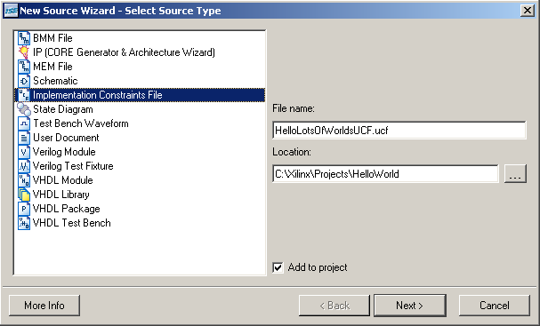
After selecting 'Next' and 'Finish' a new user constraints file will be created and automatically placed under the current top module. Select the newly created module from the Project Window, and expand the 'User Constraints' option in the Design Flow Window. Finally, double click on the 'Edit Constraints' option to open a blank file.
Your old user constraints file had the following code in it to describe the pin-out.
NET "IN" LOC = "P69" ;
NET "OUT" LOC = "P15" ;
For a bus it is slightly different. Here the individual wires of the bus are referenced using angular brackets, for example.
NET "IN<0>" LOC = "P69" ;
So now you need to do some reading from that friendly manual, to find out the pin addresses for each of the switches and the LEDs. Then fill out a line for each wire in each bus, a total of 16 entries. Hint look at page 4 of the manual. If you need more help, the answer is displayed if you push the button. An example is dislayed below, but was designed for a different FPGA. Yours may have a different addressing scheme using different letters and numbers.
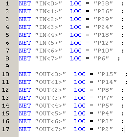
NB. Note that Switch SW0 is connected to Pin "P11" as stated in the board reference manual document, and not "M4" as wrongly printed on the board.